
Heterogeneous Integration for the AI & Automotive Era: Inside the i-Packaging™ Platform
As high-performance electronics continue to evolve, traditional chip-level packaging is increasingly constrained by system-level requirements, including power density, thermal management, bandwidth, and form factor. These limitations are particularly evident in AI computing infrastructure and advanced automotive systems, where performance scaling can no longer rely on device-level improvements alone.
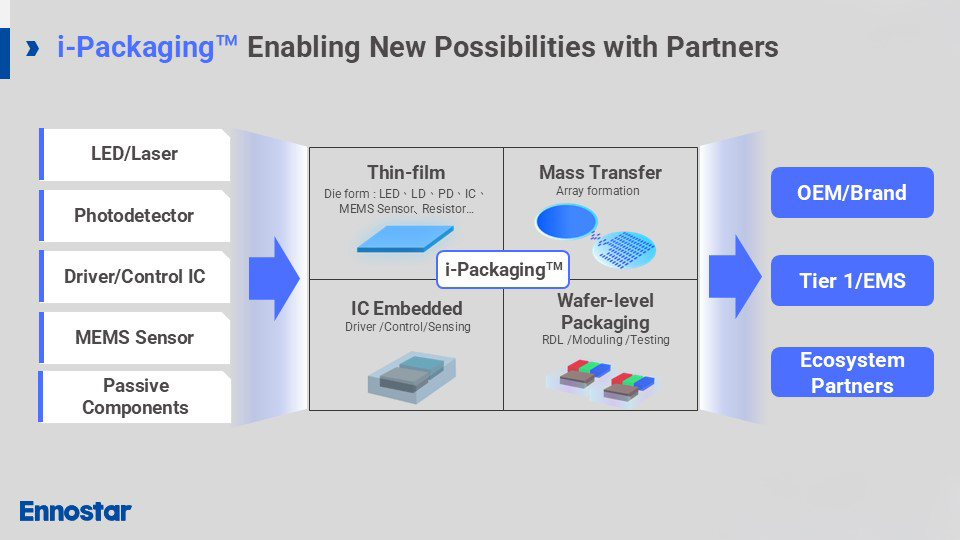
To address these challenges, Ennostar has developed i-Packaging™, a heterogeneous integration platform that rethinks how optoelectronic components are integrated, packaged, and scaled for next-generation applications.
By treating semiconductor components as modular “building blocks,” i-Packaging™ enables flexible integration of LEDs, MEMS, sensors, and ICs into compact, high-performance modules—bridging the gap between device innovation and system-level implementation.
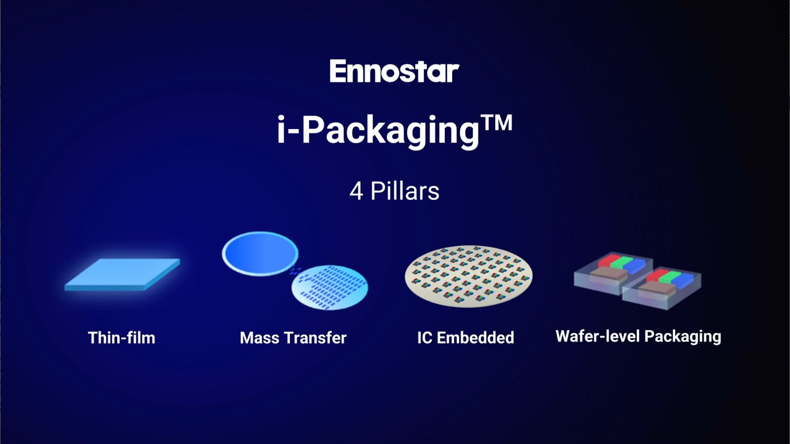
The 4 Pillars of i-Packaging™ Innovation
The i-Packaging™ platform is built on four tightly integrated technologies that collectively enable scalable, high-density optoelectronic integration across diverse applications.
1. Thin-Film Technology
The Thin-Flim Technology supports integration of R/G/B LEDs, photodiodes, MEMS, sensors, and ICs, with CoW(Chip-on-Wafer) thickness down to below 5~20um. This approach enables the availability of heterogeneous integration even when the source wafers with different diameters, minimizing NRE by eliminating the need for additional tape outs.
.jpg)
2. Mass Transfer
Advanced array formation and selective transfer techniques allow accurate pitch control while supporting scalable manufacturing. This approach balances precision, throughput, and yield, which is essential for high-volume production.
3. IC Embedded Architecture
Driver, control, and sensing ICs are embedded directly within the package structure. This reduces interconnect latency, improves signal integrity, and simplifies the overall circuit design at the module level.
4. Wafer-Level Packaging (WLP)
Through Redistribution Layer (RDL) technology and advanced module structuring, i-Packaging™ delivers slim, compact, and more comprehensive solutions compared to conventional SMT-based approaches without compromising manufacturability. It helps us realize Heterogeneous Integration with high-resolution and multifunctional module designs while maintaining high quality optical and electrical performance.
Redefining Automotive Lighting with the “Slim Core” Architecture
One of the most immediate applications of i-Packaging™ is automotive Adaptive Driving Beam (ADB) systems. Conventional automotive packaging often suffers from large pixel gaps and optical artifacts such as the “Yellow Halo” effect, limiting both resolution and design flexibility.
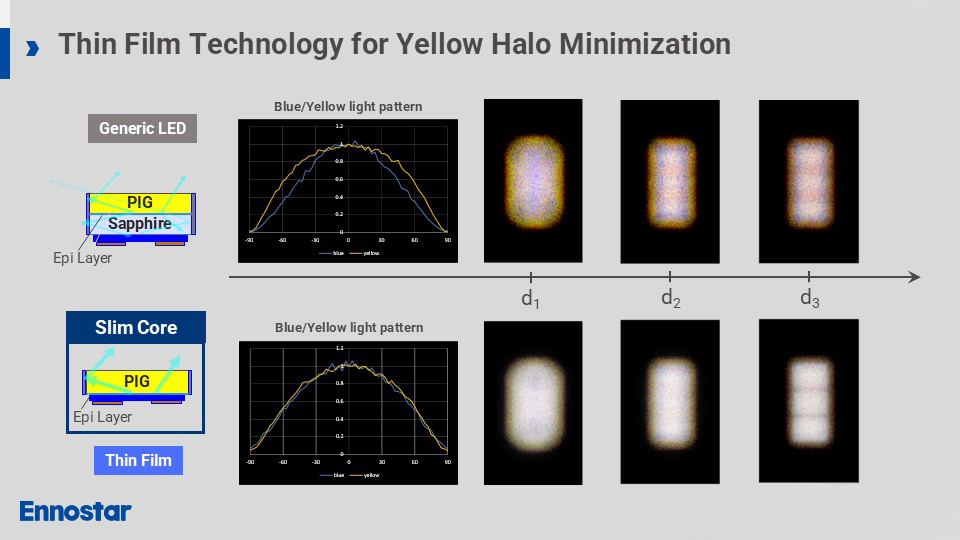
Ennostar’s Slim Core architecture addresses these challenges through:
- Yellow Halo Minimization
A combination of thin-film processing, high-reflectivity optical design, and cross-talk suppression significantly improves beam uniformity. - High-Density Miniaturization
Pixel gaps are reduced from greater than 500 µm in traditional packages to just 50 µm, enabling finer beam control and higher-resolution light patterns. Expanded Functional Capability
This level of precision enables Pixelated Ground Projection, allowing vehicles to project safety warnings, navigation cues, and customizable welcome patterns directly onto the road surface, extending automotive lighting from illumination to communication.
Optical Interconnects for AI Data Centers: Addressing Power and Bandwidth Constraints
The rapid expansion of AI workloads is driving unprecedented increases in data center power consumption and interconnect density. As electrical interconnects approach their physical limits, optical interconnects are emerging as a key technology for next-generation AI systems.
The i-Packaging™ Interposer is designed specifically to support high-performance optical integration:
- Ultra-Thin Profile
Achieves a total thickness of less than 0.1 mm, enabling compact and thin-profile optical modules. - Improved Thermal Performance
Enhanced heat dissipation supports stable operation in high-density, high-power AI computing environments. - Multiplexed Optical Bandwidth Scalability
Enables multiplexed Micro LED array architectures through i-Packaging™ integration, supporting the bandwidth density and signal scalability required by emerging Co-Packaged Optics (CPO) systems. High-Yield Precision Bonding
An array-first formation process combined with pre-screening ensures high-yield, high-accuracy bonding of Micro LED elements—critical for scalable deployment.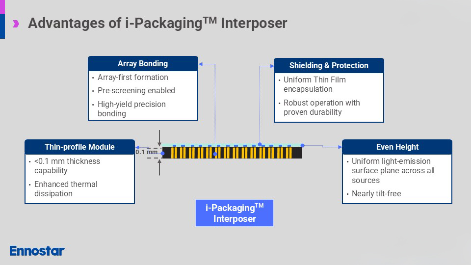
The Advantages of i-PackagingTM Interposer
Conclusion: A Scalable Platform for Future Optoelectronic Systems
The i-Packaging™ platform extends beyond conventional packaging by providing a modular and scalable foundation for heterogeneous integration. It enables partners to accelerate development across applications such as automotive lighting, AI optical interconnects, wearables, transparent HUDs, and smart appliances, while balancing performance, manufacturability, and time-to-market.
"The i-Packaging™ architecture is designed to be market-agnostic, providing partners with a stable, high-yield integration path that adapts to varying component requirements without requiring a complete process redesign."
Now, bring your "Brick Set" ideas to life! The i-Packaging™ platform is built for versatility across automotive, AI infrastructure, and intelligent sensing. We invite technology partners to collaborate with us in building the next generation of compact, high-performance optoelectronic modules.