
Touch Taiwan 2026 Report – EP2: Industrial Autonomy and High-Precision Sensing Architectures
Link copied!
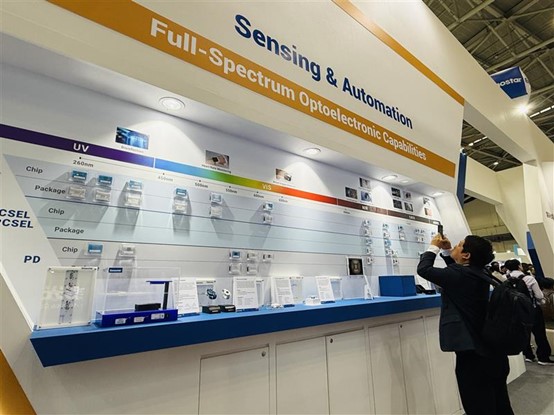
In the 3rd installment of our series, Touch Taiwan 2026 showcase underscores the critical role of full-spectrum optoelectronics in the advancement of industrial autonomy and biosensing. By leveraging a comprehensive wavelength portfolio—spanning from 220 nm (UVC) to 2400 nm (eSWIR)—Ennostar is positioning its technology not merely as discrete components, but as a foundational sensing layer for the Edge AI era.
1.Full-Spectrum Material Leadership: From 220 nm to 2400 nm
A central pillar of Ennostar’s technical roadmap is the vertical integration of III-V semiconductor materials. This mastery of the full electromagnetic spectrum enables precise solution-matching for diverse industrial requirements:
Ultraviolet (220–370 nm):
High-responsivity GaN-based photodiodes for separate UVC and UVA monitoring, essential for sterilization and industrial curing validation.
Visible to Near-Infrared (450–940 nm):
High-power blue lasers for non-ferrous metal processing and high-efficiency VCSELs for spatial mapping.
Extended Short-Wave Infrared (1300–2400 nm):
Advanced InGaAs-based detection systems designed for complex molecular analysis and non-invasive diagnostics.
2.Advanced Biosensing: eSWIR for Non-Invasive Glucose Monitoring
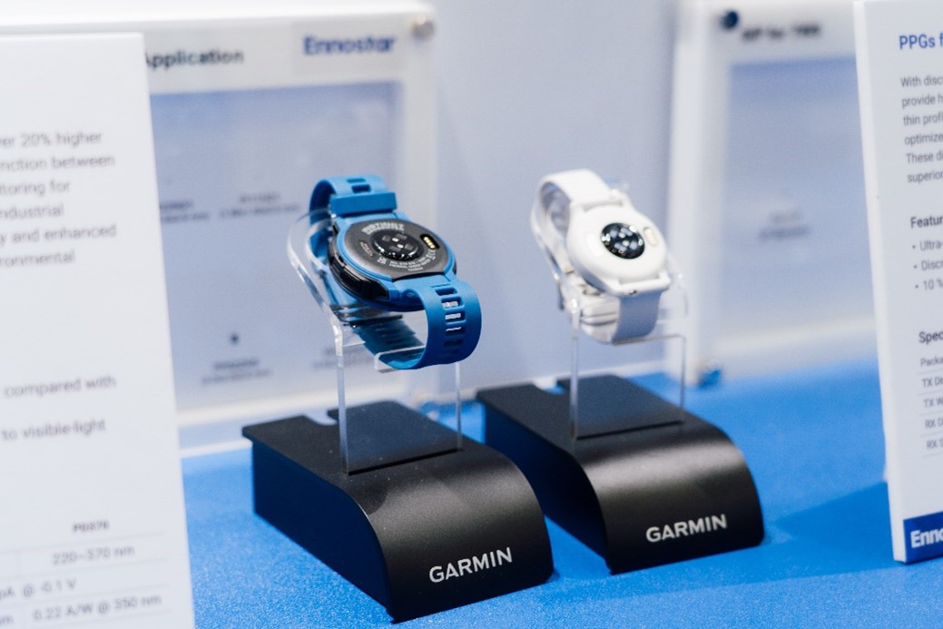
A significant architectural shift in the wearable health sector is the transition toward the eSWIR (Extended Short-Wave Infrared) band. Ennostar’s InGaAs eSWIR photodiodes (1300–2400 nm) address the historical technical barriers to non-invasive glucose measurement.
Molecular Absorption Precision:
The 2200 nm peak provides a distinct absorption signature for glucose, allowing for higher specificity compared to traditional NIR solutions.
Signal-to-Noise Optimization:
By delivering a responsivity of 1.3 A/W at these extended wavelengths, Ennostar’s architecture enables the high SNR (Signal-to-Noise Ratio) required for high accuracy in consumer-grade wearable form factors.
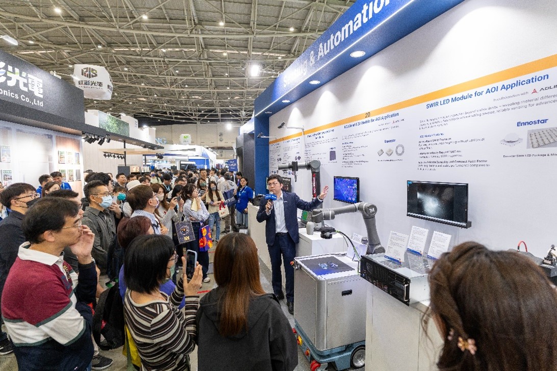
3.The Sensing & Automation Zone: Collaborative Ecosystems
Under the conceptual framework of "We Sense. We Connect.", Ennostar demonstrated the integration of optoelectronic hardware with workstation-class computing. This "cross-domain" approach is essential as industrial automation requires real-time processing of high-density volumetric data.
Ennostar presented several collaborative platforms with strategic partners:
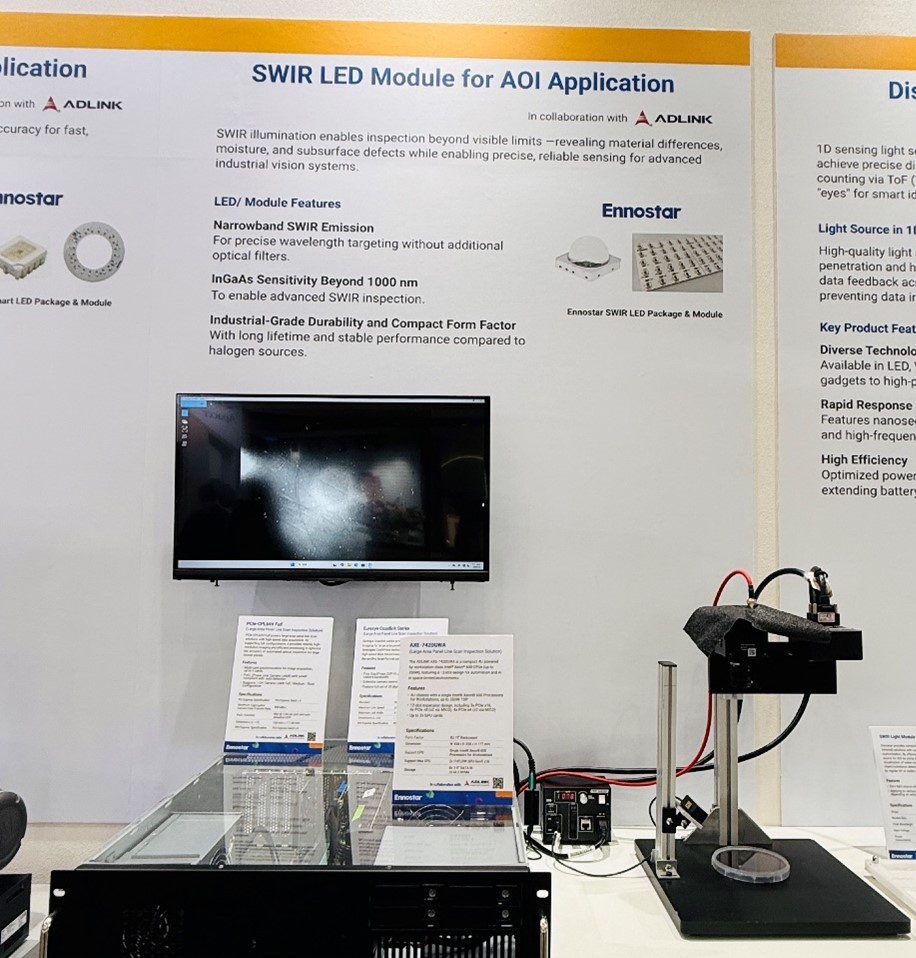
2D Machine Vision & AOI:
In collaboration with ADLINK Technology, Ennostar showcased SWIR light modules integrated with Edge AI workstations. This configuration enables the detection of moisture and material defects in semiconductor and pharmaceutical packaging that are invisible to standard silicon-based sensors.
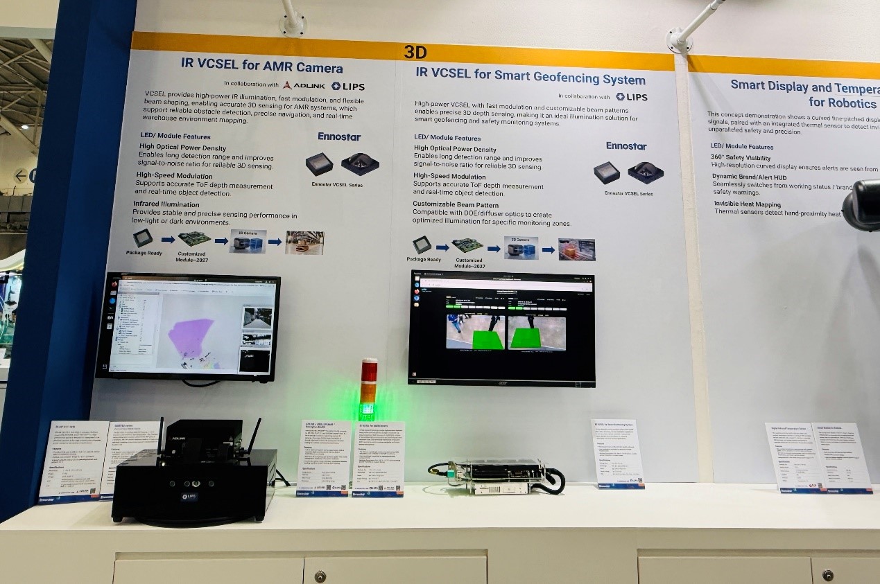
3D Vision & Navigation:
Partnering with LIPS Corporation and ADLINK, Ennostar demonstrated AMR (Autonomous Mobile Robot) navigation architectures. These systems utilize 940 nm IR VCSELs to provide high-resolution depth data, ensuring robust performance in high-ambient-light industrial environments.
Safety Geofencing:
Working with LIPS, Ennostar presented virtual safety barriers. These rely on VCSEL with high spatial uniformity and nanosecond-level modulation to define precision volumetric boundaries for human-robot collaboration.
4.Technical Specification Overview
Category | Technology | Key Specifications | Primary Application |
Next-Gen Solutions | 1310 nm PCSEL | 500 mW / 1.5° Divergence Angle | Long-range LiDAR / Automotive Safety |
InGaAs eSWIR PD | 1300–2400 nm / 1.3 A/W Responsivity | Non-invasive Glucose Sensing | |
Commercial Roadmap | IR VCSEL (AMR) | 940 nm / 3W - 7W Output @ 4.5A | 3D Depth Sensing / AMR Navigation |
Blue Laser Chip | 450 nm / 6.0W Output | EV Battery Welding / Metal Processing | |
Sensing Portfolio | UVC/UVA PD | 220–370 nm / <10 pA Dark Current | Industrial UV Source Monitoring |
Biomedical | Digital IR Temp | ±0.2°C Medical-Grade Accuracy | Wearable Vital Sign Monitoring |
Conclusion: Toward an Integrated Sensing Architecture
The Touch Taiwan 2026 series confirms a significant industry trajectory: optoelectronics are evolving from passive components into active, intelligent interfaces. Following our analysis of Pixelated Automotive Architectures (EP1) and Scalable Data Center Interconnects (EP3), this third installment highlights the convergence of full-spectrum sensing and AI-driven automation. Ennostar remains the primary vertical integrator, bridging the gap between semiconductor physics and high-precision industrial applications.